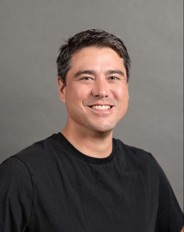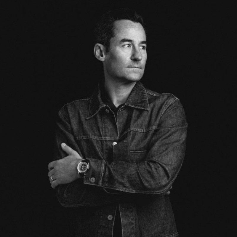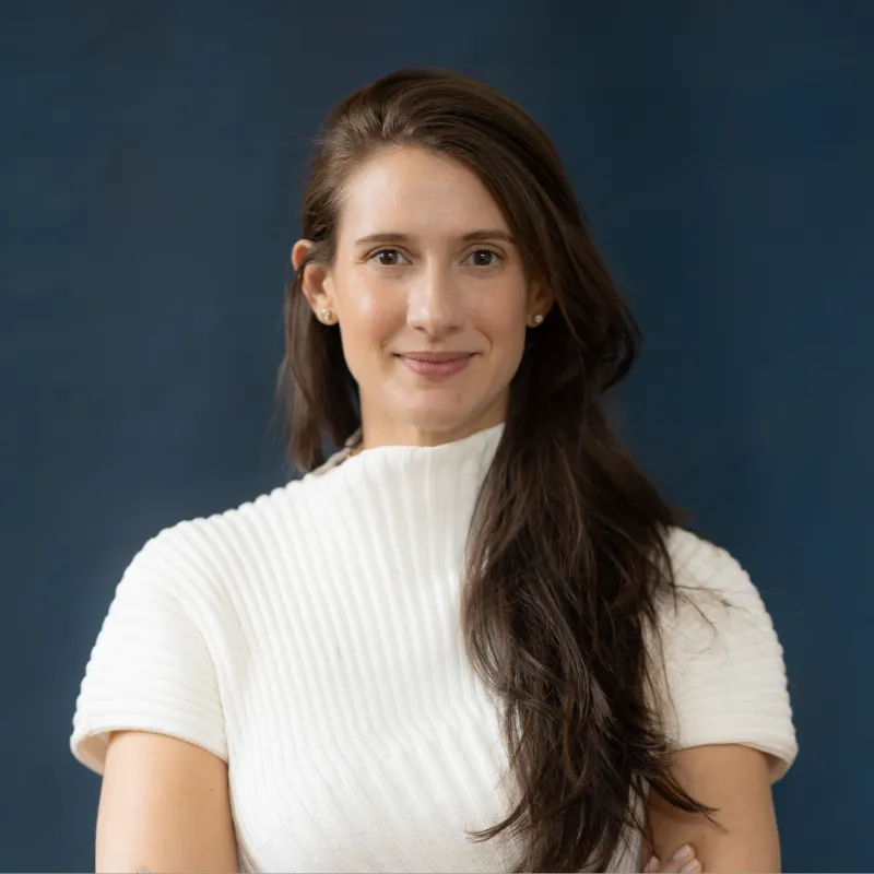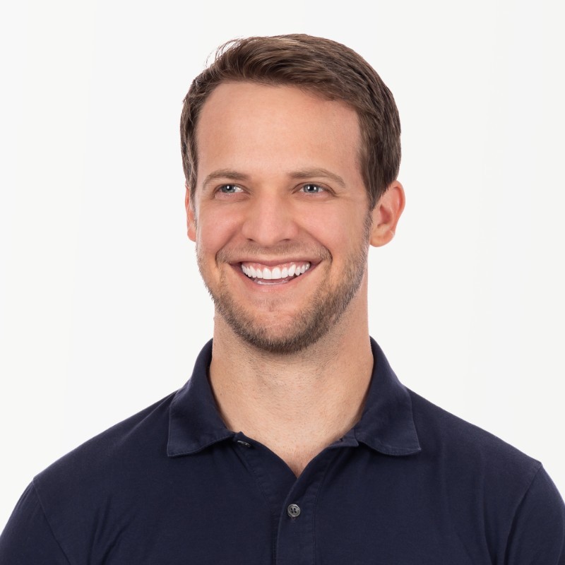



Tarun Verma joined Silicon Catalyst in 2015 as its first employee after spending about 24 years at Altera leading packaging work, and that background shows up in how he talks about semiconductor investing, especially his focus on packaging and chiplets as a way to make chip design more affordable for startups. He also looks for companies that fit into the existing manufacturing ecosystem, works to cut the cost of early prototyping so founders can move faster, and points to practical tools—like test equipment, FPGA prototyping, and facilities—as key pieces for helping semiconductor startups grow from early research into real products, both in the U.S. and internationally.
About their Fund

Silicon Catalyst

Sectors
Chips, Deeptech / Hardware, AI, Materials, Medtech
Rounds
Avg Check Size
Notable Investments
Silicon Catalyst is the only accelerator focused exclusively on the global semiconductor industry, giving startups working on chips, chiplets, materials, silicon photonics, MEMS, sensors, life science, and quantum access to a semiconductor-specific stack of foundry access, EDA tools, IP, packaging, and testing worth millions of dollars, plus a 24-month incubation program, strategic partners like TI, Arm, and NXP who help select and work with startups, and its own investment arms, Silicon Catalyst Angels and Silicon Catalyst Ventures. It operates this model through localized programs in the UK, EU, Israel, Japan, Australia, and Malaysia, connecting local startups to Silicon Valley networks and mentors, and has built an ecosystem that has engaged with over 1,500 semiconductor startups, admitted more than 150, and facilitated over $150 million in in-kind support, $600 million in venture investment, and $100 million in grants.
Other partners at the fund
Notable Fund
Investments
No items found.
Sheets they're in
No items found.
Sheets they're Fund is in
No items found.
Is this information out of date? Let us know
Popular Investors
investor name
Active in
Rounds
Avg. Check
Links


Deeptech / Hardware

Robotics

Biotech
+
12
View more in profile...
Unknown
Pre-Seed - Seed
Unknown
$400K - $2M
Unknown


Defense
Deeptech / Hardware

Energy
+
7
View more in profile...
Unknown
Pre-Seed - Series A
Unknown
$100K - $5M
Unknown

Defense
Deeptech / Hardware
Energy
+
7
View more in profile...
Unknown
Pre-Seed - Series A
Unknown
$100K - $5M
Unknown


Biotech

Health
Deeptech / Hardware
+
2
View more in profile...
Unknown
Pre-Seed - Seed
Unknown
$250K - $2M
Unknown





Climate
Deeptech / Hardware

Materials
+
4
View more in profile...
Unknown
Pre-Seed - Seed
Unknown
$400K - $1.5M
Unknown

Deeptech / Hardware
Robotics
Biotech
+
7
View more in profile...
Unknown
Pre-Seed - Seed
Unknown
$400K - $2M
Unknown

Deeptech / Hardware
Robotics
Biotech
+
2
View more in profile...
Unknown
Pre-Seed - Seed
Unknown
~$750K
Unknown


Fintech
Deeptech / Hardware

Devtools
+
2
View more in profile...
Unknown
Pre-Seed - Series A
Unknown
$250K-$1M
Unknown


Or automatically find your investor matches
Upload your pitch deck to get your best investor matches in minutes.
Reveal the very best VCs to pitch for your startup
Get matching investors' email addresses
No ads. No catch. Free from VC Sheet.
Thank you! Your submission has been received!
Oops! Something went wrong while submitting the form.
Success. Check your email in 5 minutes.